Friday 26 June 2015

BRUSHED DC MOTOR SPEED CONTROLLER


We often need to control the speed of DC Brushed motor in many situations.The commercially available speed controller are very costly so why not make a cheap motor speed controller easily at home.The main idea behind controlling the speed of DC Brushed motor is that the RPM or speed of Rotor of DC motor is directly proportional to the square of voltage applied across the terminals of the dc motor, hence by decreasing or increasing the voltage across the terminals of the motor we car easily increase or decrease the speed of the motor.Now question arises how to vary the voltage across the terminals of motor. A circuit can be designed to vary the voltage across the terminals of motor using some transistors and some potentiometer. Here is the circuit diagram-

The above circuit is the DC motor speed controller circuit in which two transistors are connected in dalington configuration. Here the list of components used-
:: one 10k ohm Resistor (R1)
:: one 10k ohm potentiometer or preset (RV1)
:: one 10 ohm resistor (R2)
:: one 2N3904 Transistor (Q1)
:: one MJE13003 Transistor (Q2)
:: one Brushed DC motor
:: connecting wires
:: Perforated or general board for mounting components
:: solder and soldering iron
The darlington configuration of the two transistors is obtained by connecting the Emitter of Q1 with the Base of Q2 and connecting both Q1 & Q2 collector together. Now the obtained configuration is darlington configuration which behaves as a single transistor whose base is the base of Q1 and the emitter is the emitter of Q2 and since the collector of both transistor are connected therefore it is the joined collector of the single behaving transistor as shown in the circuit diagram above. The most important property of a darlington configuration is the Hfe product property.
The Hfe of the dalington pair of the transistor as a whole is the product of the individual transistor's Hfe. Hence we get a large output for small change in base current of Q1. Also the 2N3904 is capable of handling about 500 mili amps of current also it get very hot when operated at extreme positions hence to eliminate this 13003 (Q2) transistor is used with 2N3904 (Q1) in dalington cofiguration in which the 13003 will sink all the current passing through the motor as it is capable of delivering maximum current of 3 amps. , Normally motor needs less than 1 amp. . If your motor is of higher current rating then you can replace 13003 (Q2) transistor with another suitable transistor which can deliver higher current then 13003 like 13007 ,etc,.
Now the darlington pair is properly biased by using voltage  divider  biasing  technique with the help of a 10k ohm resistor and a 10k ohm potentiometer or preset. The potentiometer or preset is a device whose resistance can be varied in some specified limits by rotating the knob of potentiometer or by rotating the wiper of preset using screwdriver. Below is a potentiometer.

The potentiometer's knob will be used for the controlling speed of motor by rotating it. The middle terminal of the potentiometer or preset is the variable resistance terminal which is connected to the base of the transistor Q1 and other terminals are used for completing the biasing circuit of the darlington pair.The motor is connected at the terminals A and B as shown in the circuit.The emitter of Q2 is grounded through a 10 ohm resistor to regulate the flow of current through the motor. The current flowing through the motor  is the sum of collector current through Q1 and Q2 transistor. But large quantity of current flows through the 13003 transistor. A small change in the value of current through the transistor's base Q1 brings large change in current and hence voltage across motor. So by rotating the knob of the potentiometer ,the resistance below R1 changes and hence the voltage across RV1 lower changes linearly consequently the voltage at the base of transistor Q1 changes which changes the base current of Q2 and hence voltage across Terminals A and B changes. Which changes the speed of the DC motor connected at terminals A and B.
Hence in this way the speed of the Brushed DC motor can be varied by just rotating the Knob of the potentiometer in the Circuit.
For making the physical circuit on pcb just place all the listed components in their proper place and connect as shown in the circuit diagram.For details about making pcb of circuit click here.

Wednesday 22 October 2014

12 V DC POWER SUPPLY


Today I am going to make here a 220 Volt AC to 12 Volt DC  Power supply.

For that we must be familiar with the conversion of  high voltage AC to low Voltage AC.A transformer is used for the conversion, which is the combination of two coils mutually coupled together using a ferrite core, Which is a soft iron core.One coil is of large numbers of turns with high resistance of small diameter of copper wire, which is called high voltage coil and another coil is of low resistance ,low number of turns but with comparatively large diameter of copper wire,which is called low voltage coil.
TRANSFORMER TEST-
Before using the transformer we must know which coil's terminals should be connected to mains or circuitry.It is important since this knowledge would protect your home wiring as well as protects your transformer  from being burned or damaged.
Now have a multimeter  (analog or digital) with you and set it to ohm measurement,now test each coils terminals,see that what readings you get.
If you are getting a reading in few kilo-ohms then it must be the high voltage coil or primary coil.
If you are getting a reading in only ohms then it must be the low voltage coil or secondary coil.
Also test for the shorting of the coils by checking the resistance of both the coil is infinite or not,If not then the transformer is faulty, just change the transformer.

Also test for the coil and core resistance is infinite or not,If so then be aware that you can get shock if you don't take care of it.It is recommended that you must change the transformer in such condition.
BUILDING THE DEVICE-
Here is the list of components-
:: Four 1N4001 diodes
:: one 9-0-9,500mA transformer
:: one LM7812 IC
:: one 470uF,50v Electrolytic capacitor
:: one 10uF,25v Electrolytic capacitor
:: one 0.1uF ceramic capacitor
:: wires
:: shoulder and shouldering iron
:: A perforated copper board or a copper clad board with 5cm By 5cm                  dimensions.  
:: A 10 cm by 10 cm cardboard
Make a bridge rectifier (see here how to make bridge rectifier) on the perforated board now take the transformer secondary or low voltage coil terminals as the rectifier AC input.The 9-0-9 has three terminals of the low voltage coil,leave the zero potential or common terminal of the coil and take the other two terminals.Always remember that a transformer output gives an AC voltage which has no polarity so don't worry of the connection at the rectifier input,it can be connected at any polarity as the input to rectifier.
Now the output of the bridge rectifier is always fluctuating DC, for knowing the polarity test it with the multimeter.You can also know the polarity by seeing that the same p terminals connected together will have negative output and vice-versa in the bridge rectifier.


Now after knowing the polarity, connect the 470uF capacitor in parallel to the bridge rectifier output.Before connecting also see the polarity of the electrolytic capacitor and connect with the same polarity as the bridge output.The black line near the terminal shows that it is negative terminal.
If the electrolytic Capacitor is connected with wrong polarity then the capacitor may explode.Also connect another 10uF electrolytic capacitor in parallel with the 470uF capacitor with correct polarity.

Now connect the positive terminal of the capacitor to the input or first terminal of the LM7812 IC and other terminal to the ground terminal or second/middle terminal of the IC. Now take the output at third/Output terminal of the IC w.r.t. the ground terminal.For stability Connect 0.1uF capacitor in parallel to the output terminal and ground terminal.Take the output across the 0.1uF capacitor.
Now fit all the circuitry on the cardboard and use it for any electronic application, Which requires 12v dc and 400mA of current.For high current applications just add a heat sink to the LM7812 IC.
You can also mount the components on a copper clad board PCB (See here how to make PCB).

Here are some pics of the Device-


Saturday 12 July 2014

HOW TO MAKE PCB OF AN ELECTRONIC CIRCUIT USING EXPRESS PCB

Hi friends today i will tell you about pcb making of an electronic circuit. To temporary make the circuit some persons use perforated boards to mount and shoulder the components. But to make permanent circuit we use copper clad board so as to ensure less wear and tear with the pcb. Some of you might have seen the pcb inside various electronics equipment e.g., T.V. , Radio, etc. We will make pcbs similar to that with perfect outline of the tracks as it has been manufactured from a company. Now first of all you must know the circuit diagram of electronic gadget you are going to make. The circuit schematic is drawn on the paper with the pin connections of different terminals of  electronics  components. The circuit diagram  helps   us for accurate making of pcb layout with right pin connection.Now the express pcb software is used for drawing the schematic in express SCH portion of the express pcb software and after making,Its printouts is taken and the circuit schematic is obtained in this way.For making the circuit schematic you must install the express pcb software (Download here free).Now after installation you will find two icons viz. expressSCH and expressPCB.The former is used for drawing the schematic,  Now double click  the the former icon and a window will appear showing various tools and drawing area.You can choose any of the ICs and electronic component from the menu.The component Menu comes when you click on the analog icon on the tool bar. Then you choose the required component or IC. Now after choosing the correct item you can place it on the work area.The component Menu contains various ICs with their part numbers and company name also like Texas instruments     SN75160, Linear Technology LT1070, Atmel Microcontrollers, Microchip PIC microcontrollers series ICs,and many more are there in the component Menu.You can choose your desired ic of which you are going to make the circuit.The ICs contains all the associated Pin with names Labeled. If the component is not listed in the Menu Then You can create your own component using Various tools in the tool bar, these component are at no.9,10,11 Position from the upper most tool.Get the information of making the custom component in the Quick start Guide of the Express SCH. You can connect the various components pins using the Connecting wire Icon from tool bar at left.Now according to the Datasheets and application notes of the components and ICs make the correct connection with wire tool. When the circuit is complete you can print the whole circuit on paper and obtain the schematic, and save the .sch file. Now double click on the express PCB icon and you will find there a toolbar,Menu bar,In The toolbar you will find a component Menu tool in the shape of an IC. You can then select the proper component and place it on the work area.Different connectors and different IC packages are available such as SOIC package,QFN package,DIP Package ,etc.This Creates a versatile ways of designing your pcbs. Now select the Wire tool for connecting different pins of the components, Also you Can link your .sch file in the ExpressPCB for Pin Connecting aid.However it is recommended in large circuit since the chances of wrong pin connection are high as compared to small circuits.It is not necessary to link the .sch file to ExpressPCB also it is not necessary that you draw schematic in ExpressSCH  for small circuit you can take a look at pin connection by hand made schematic. For linking the .sch file go to File option in the Menu bar and select 'Link schematic to PCB' .You can also configure the track width and it curvness.It is recommended to use keyboard keys for proper placement of component and wires for a perfect layout.Also the thermal pad option is available and the top layer and bottom layer option is available.You can make the custom components if it is not available in the component list. For procedure of making the custom component see the 'Quick guide of ExpressPCB' .Now after completing the layout Go to print option in the File option in Menu Bar or use short cut keys ctrl+P. Here  If you have make the pcb layout in both top layer and bottom layer then you can choose either one or both at a time.You must mention or choose the paper size for printing like A4,A3 ,etc.The paper that you use for printing must be a Butter paper or a magazine paper and the printer that you use must be the Laser printer.If you Don't have a laser printer then select in the printer option 'Windows XPS document writer'  and click ok. You will get a .xps file which you can take in pen drive and go to a photostat shop or cyber cafe that have a laser printer and print the layout on the butter paper or magazine paper. Always see the component datasheet for the proper size of the package of ICs or component you are going to use in your circuit.Also Read the Quick Guide of the softwares.Here is the Pcb Layout Of a Transmitter and Receiver Circuit Using HT12D and HT12E and RF Modules in ExpressPCB.


Here is the pcb layout of Transmitter and Receiver Circuit Using HT12D and HT12E and RF Modules which is ready for printing.


The above layout is from .xps file of the circuit.Now after printing the .xps file on Butter or magazine paper.Keep the following list of items ready for pcb making-
:: Copper clad board   (desired size)
:: Ferric chloride         (depending on size of board, dissolve 10gm in water for 50 by 30 copper clad board)
:: Electric Iron
:: Thinner
:: permanent marker  (for error correction) 
Now take the copper clad board of the size a little greater than the pcb layout.Now cut out the extra paper in the margin of the printed paper and then put in over the copper clad board where the copper is present with the printed side touching the copper surface.Before placing the paper rub the copper side of copper board with the help of scotch-brite available in market and clean the board with the help of cloth.Now pre heat the clothing iron for five minutes then place it over the magazine or butter paper below which the copper board is present.And apply lot of pressure and heat for 10 minutes and then take the board carefully since it is hot.You will see that the paper has sticked to the board then wash the paper with lot of water and remove the extra paper.You will see that the toner has been transferred to the board i.e. the whose layout has been transferred to the board.Also verify the design that all tracks are right or not,if you find any incomplete track then correct it by using permanent marker Keep the ferric chloride solution ready and dip the printed board in the solution for fifteen minutes (Eaching Process). Here are some snapshots-

Below is the Dual H-Bridge for Motor direction control used in remote control car.Its layout is not shown here.

Below is the PCB Layout of above circuit in express pcb.

Here is PCB layout from .xps file.


Here is the PCB in Ferric Chloride solution-


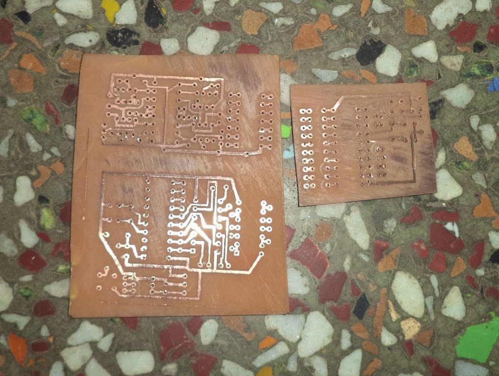
When Fifteen minutes has completed take out the pcb from the solution with the help of gloves and wash it with water.Now clean the pcb with thinner you Will notice that the extra copper has been removed and your pcb is ready for drilling.Drill the holes using hand drill or stand still drill at appropriate places where the components are to be placed. Use appropriate size of drill bit normally use 1mm bit.After drilling your pcb is ready to be used for placing components and shouldering.But before making the PCB layout of the circuit test the circuit on a breadboard.Here are the pcbs of the layout shown in this article.
Below is the H-Bridge circuit PCB.

Below is the Transmitter circuit PCB.


Below is the Receiver circuit PCB.

You can use the vast varieties of PCB designer software Only the difference lies is the operation of software but the procedure is same printing,transfering,eaching process etc. are same.Be careful with Ferric Chloride since it is highly corrosive.It is recommended to use gloves for treating with Ferric Chloride.

Thursday 12 June 2014

HOW TO MAKE A REMOTE CONTROL CAR


A Car consists a motor to give it forward and backward motion and its extended version would consist of another function of left and right motion which also require second motor. Therefore a car can have a minimum of Four Functions viz. Forward(Turbo), Backward, Left and right motion. The forward motion of the car is also termed as turbo because in this motion the driver takes full advantage of car as car lover already know.The car motor is powered by a dry 12v or 6v battery so that maximum torque and speed combination is developed in the motor.If the car is wired then it is easy to make it and run it but you have to move with the car also and there is always a chance of wear and tear of the car wire control of the car.The wired car range of running forward is less as compared to wireless car.It cannot move to farther distance like wireless car ca do. Hence there is a need of having wireless remote control car but it market cost is quite large, why not make your own cheaper wireless remote control car with some electronics knowledge and component available in the market are cheaper then the actual remote control car. First of all you should have the knowledge of various  electronics components  like transmitter and receiver module. In india 315 Mhz and 433 Mhz band is allowed as general purpose frequency band for common people use.Hence transmitter and receiver module are available in this range of frequency bands.The transmitter and receiver module are nothing but premade pcbs by using different amplifier stages and op amp ic and totally depend upon manufacturer.The transmitter module is usually smaller in size than receiver module and have Four terminals or pins  viz. Vcc , Data in, Ground and Antenna.The Receiver Module also has four main terminals Vcc, Ground, Antenna and Data out.
Transmitter module (left) and Receiver Module (right)

They work on ASK  (Amplitude shifting Keying) Modulation.It is a type of digital modulation. ASK is a form of Amplitude modulation which represent digital data as variation in amplitude of a carrier wave.The amplitude of the carrier changes according to the digital baseband signal.

I recommend you to study the transmitter and receiver module datasheet once only to know about its working and its rating.You can buy the modules either from eBay or from Delhi chandni-chook electronics market (for indians).I have bought three pair of modules worth Rs.525 (each Rs.175), from Shop no-594.  
Now the next thing you must know about is the Encoder HT12E and Decoder HT12D ic which are most important part of the RF circuit.The encoder ic is the ic for taking input through it four pins viz. 10,11,12 and 13 pins of the ic These pins are the data pins and denoted by  AD8 ,AD9, AD10 ,AD11.These pins have to be connected to  ground through push buttons.The Address pins 1 to 8 is used to provide the address of the transmitter and the Decoder ic must have same address so as to interact with the transmitter .The encoder in simple words is the multiplexer which encodes or multiplexes the signal along the same band of channel.It increases the total capacity of the channel band.They are available as 4 bit encoder.Here is the pin diagram of HT12E with transmitter module. The Dout is the four bit data with the 8 bit address multiplexed with it.The encoded signal is given to transmitter module Data in pin for the transmission the the ASK signal.

Now let us talk about HT12D ic.It is a decoder ic and is used to demultiplex the received data from receiver module.The HT12D ic does the reverse of HT12E ic.It decodes the received data into useful four bit information for remote control application.The decoder address pin connection must be in same configuration as that of encoder ic,otherwise it may not decode the received data into useful information.Here is the pin diagram of HT12D ic with Receiver module.


The receiver module receives the signal and give it to the Din pin of the decoder ic.The decoder ic decodes the data given and provide the four bit useful data at pin no. 10,11,12,13.Which is used for remote control application.
The data is serially transmitted and received.
Now the next ic you must be familiar of is the Quadruple Half H-Drivers Ic which is the LD293D Ic.It has four H-bridge Drivers and is used in controlling the forward and backward motion of motors.You Must read the datasheet of all the ICs discussed in the article.Here is the pin diagram with application.


Th Driver Ic has 16 pins in which pin no. 4,5,12,13 are ground of the Ic and pin no.16 is the ic supply voltage and Pin no.8 is the motor supply voltage.Pin no. 3 and 6 are enable for the motor bridge circuit and must be connected to the +5 volt supply so as to enable the H-bridge.Pin no. 3,6 and 11,14 are the output for motor terminals.Pin no.5,7 are used for controlling the forward and backward motion of the motor connected at pin no.3,6 and pin no.10,15 are used for controlling the forward and backward motion of the motor connected at pin no.11,14.
The next Ic is the 5 volt supply Ic which is LM7805 ic.It takes battery terminal voltage input greater than 7 volt and less than 36 volt And convert it into 5 volt.Here is the circuit diagram.


Now we have Enough Knowledge about the components to be used.Here is the List of components required For making the Remote control car.
:: LM7805   IC                                                           2nos
:: LD293D   IC                                                           1nos
:: HT12D     IC                                                           1nos
:: HT12E     IC                                                           1nos
::315Mhz Transmitter and receiver Module Pair       1nos
::9v dry battery                                                             2nos
::Copper clad board                                      50cm by 50cm
::Cardboard                                                   50cm by 50cm
::DC Motors                                                                 2nos
::Gears                                                                As requred
::Feviquick                                                                   10ml
::Ferric chloride                                                         30gms
::water in plastic bucket                                            
::Hand Drill
::Express Pcb software installed on your computer.
::Magazine paper
::Laser printer
Here is the block diagram of the remote control car --
The motor 1 is the steering motor and motor 2 is the engine power motor.I have used various stuff to design the hardware of the car and it will be discussed later. 
Now First of all Make the following circuit on Express pcb and then justify all the pin connection according to the given circuit diagram--


For making the pcb layout you must be familiar with express pcb software.It is the software used for designing the pcb layouts and it is freeware, you can download it from Here.It has two parts one is the Express SCH and other is Express PCB.The former is used to make the circuit diagram and then it is linked to the latter which is used for designing the pcb layout.If you don't want to make the circuit diagram in SCH then no matter you have to justify the layout in PCB design.
Now print the layout on a butter paper or a magazine paper with the help of laser printer.If you don't have a laser printer then most of the photo copy shop have the facility of laser printing then you must go there with the .xps file in flash drive and have the printed layout on butter paper or magazine paper.
Now you should cut the copper clad board with the help of a cutter of the size of layout and then cleane the copper side of the board with the help of scotch brite pad.Now further clean it with dry cloth and then put the printed side of paper on the copper side of board touching it. Now pre heat the cloth iron and then apply the heat and pressure to the board and paper using the iron for 10 minutes.You will observe after 10 minutes the paper has sticked to the board, now wash the board paper using water,you will see that the layout has transfered to the board and then dip it into the ferric chloride solution for 15 minutes. Now take out the board after 15 minutes and wash it using water.Now again wash it using thinner or kerosene oil, you will see that the pcb is ready to be drilled. Now using hand drill or stand still drill wit 1mm bit pierce the holes at appropriate places on the board for mounting the components.
Now according to the circuit diagram put appropriate components on their respective places and shoulder them using iron and paste and shoulder.Add the power supply and fix all the components pcbs and car hardware and your car is ready to use.
I have used the Lm7805, LD293D from Texas instruments and ST microelectronics.HT12E and HT12D from Holtek. 
For making the car hardware or chasis you must cut the appropriate size of the card board and the using the pads from telecoms companies which come with the SIM card, make all the support for the wheels and design the steering system as shown in fig. and then fit the motor and gears train to get more torque. And make all the connections,Your card is ready to run.
Here are some snapshots of car. 


Friday 2 August 2013

HOW TO MAKE AN AUTOMATIC STREET LIGHT USING 555 TIMER IC

Hi friends today i will tell you how to make an automatic street light using LM555 timer ic. The material required are as follows:- 
:An LM555 ic
:A 50 Kilo-Ohm Potentiometer
:An LED (white or green)
:FeCl3  Solution
:4 by 4 copper clad board.
:An LDR
:Regulated DC Power supply(+6 Volt)
:Permanent marker
:Hand drill
The circuit diagram of automatic street light is as follows:-

Made by marker


The pin no. of  IC not shown here is not in use.The adjacent picture is the pcb design of the circuit which has to be made by marker  on copper clad board.The holes on the copper clad board must be properly drilled at right place with the help of a mini hand drill.The bit used in drill must be at most .5mm dia. After marking the pcb ,it must be dipped into FeCl3  solution properly with care.Now the properly eached(cleaned) pcb is as follows:-

Here is the properly drilled PCBs. Now insert the proper terminals of a particular components in proper holes of pcb. Connect the wires with supply not more then 6volts and 500 ma.Here is the automatic street light :-

Note: positive supply is given to 8th pin no. of ic 555 and negative supply is given to 1st no. pin of the ic.
Also see the following portable model of automatic street light--
http://electronicsprojectsforfree.blogspot.com/p/blog-page.html

Here is the video:-

Friday 12 July 2013

HOW TO MAKE A BRIDGE RECTIFIER

Hi friends today i will tell you how to make a bridge rectifier.
Here is the list of essential components required:-
:Four IN4001 diodes,
:5cm by 4 cm copper clad board(CCB),
:FeCl3 (20 grams),
:Permanent marker
:Connecting wires (insulated),
:Shouldering iron and Shoulder with flux paste,
:One 470 uf,50 volt electrolytic capacitor,
:Multimeter for Voltage testing.
First we go through the schematic diagram of bridge rectifier  as shown :-

As we can see that the diodes are connected together in a particular pattern.There are four junctions formed after connecting the diodes in which two junctions are obtained by joining like poles or terminals of the diodes while others are obtained by joining dissimilar  poles or terminals.
There are two terminals of a diode one is p-type and other is n-type. A diode is that device which allows current to flow in only one direction and blocks current in other direction.
A diode is represented as shown:
The arrowhead pointing towards a line is the cathode means it is n-type material and the tail of arrowhead is the anode i.e. p-type material .But in practical purposes a diode is in the shape of a grain seed so to identify the cathode terminal a black line is marked adjacent to the cathode terminal as shown.


Now to make PCB of the bridge rectifier we have to make the following design on the copper clad board (upper side of CCB) using a permanent marker diligently.Do not over draw the copper clad board surface.Make the holes as shown using hand drill with 1mm bit.Now to make the proper connections the excess copper i.e. unmarked copper has to be removed.


To remove excess copper a high corrosive substance FeCl3 is used.The ferric chloride solution can easily dissolve the excess copper on the PCB. So to do this the PCB is dipped into ferric chloride solution obtained by dissolving 15 grams of ferric chloride to 200ml of water.
The PCB is dipped with proper care as ferric chloride is highly corrosive substance and can harm our body skin.It is dipped for 15 minutes.
After 15 minutes we can now see that the excess copper is removed and our PCB is partially ready.With the help of water wash the PCB and with thinner remove the marker ink.
Insert the proper terminals of components in their respective holes and shoulder each terminal with copper clad board using shouldering iron and flux paste.
Here is the Bridge Rectifier:-


Note:-
Always connect negative terminal to the cathode of electrolytic capacitor otherwise it will bust. 
You can also transfer the circuit design to the PCB by using laser printer.Just print this design on a magazine paper using laser printer and put the printed  surface of paper in contact to the copper clad board and put the cloth iron on it so as to give heat.Consequently,the design is transferred to the copper clad board and the rest of the process is same as explained above.

Tuesday 30 April 2013

HOW TO MAKE A 5 VOLT VOLTAGE REGULATOR

Hi friends today i will tell you how to make a 5-volt voltage regulator.
 ::LIST OF MATERIALS REQUIRED--
:A three terminal positive 5 volt voltage regulator ic ,i.e.,LM7805 ic
:A copper clad board (4.5cm by 6.2cm)
:Ferric chloride,FeCl 3    (!caution-highly corrosive substance) 
:Connecting wires
:Two 10uf capacitor ,One 1000uf capacitor,One 0.1uf capacitor ( all of 25volt and 85'C )
:Four Diodes IN4007
:A 0-18 step down transformer 500mA
:Shouldering iron and shoulder with flux paste. 
:Multimeter ( For measuring o/p voltage )


::PROCEDURE--
:Make the following design of copper clad board either with the help of using hand marking with the help of a black permanent marker (or nail polish) Or by printing the design on butter paper using laser printer and then transferring it to the board with the help of heating   (using iron).


:Place the marked board into the solution of 'ferric chloride' .After 20 minutes remove the board from solution and then first wash it with water and then with thinner.(Be careful !  Avoid ferric chloride direct contact to your body parts)
:Now place the component as shown in the figure and shoulder each and every terminals of component to the copper plate.
:Join the transformer Secondary coil to  where 18 v ac is written on the pcb (as shown in fig.).
:Now you can take o/p across 0.1uf capacitor which comes out to be 5 volt.
:You can easily charge your cell phone with this voltage output.