Hi friends today i will tell you about pcb
making of an electronic circuit. To temporary make the circuit some persons use
perforated boards to mount and shoulder the components. But to make
permanent circuit we use copper clad board so as to ensure less wear and tear
with the pcb. Some of you might have seen the pcb inside various electronics
equipment e.g., T.V. , Radio, etc. We will make pcbs similar to that with
perfect outline of the tracks as it has been manufactured from a company. Now
first of all you must know the circuit diagram of electronic gadget you
are going to make. The circuit schematic is drawn on the paper
with the pin connections of different terminals of electronics
components. The circuit diagram helps us for accurate making
of pcb layout with right pin connection.Now the express pcb software is used
for drawing the schematic in express SCH portion of the express pcb software
and after making,Its printouts is taken and the
circuit schematic is obtained in this way.For making the circuit
schematic you must install the express pcb software (Download here free).Now
after installation you will find two icons viz. expressSCH and expressPCB.The
former is used for drawing the schematic, Now double click the the
former icon and a window will appear showing various tools and drawing
area.You can choose any of the ICs and electronic component from the menu.The
component Menu comes when you click on the analog icon on the tool bar. Then
you choose the required component or IC. Now after choosing the correct item
you can place it on the work area.The component Menu contains various ICs with
their part numbers and company name also like Texas instruments
SN75160, Linear Technology LT1070, Atmel Microcontrollers, Microchip PIC
microcontrollers series ICs,and many more are there in the component Menu.You
can choose your desired ic of which you are going to make the circuit.The ICs
contains all the associated Pin with names Labeled. If the component is not
listed in the Menu Then You can create your own component using Various tools
in the tool bar, these component are at no.9,10,11 Position from the upper most
tool.Get the information of making the custom component in the Quick start
Guide of the Express SCH. You can connect the various components pins using the
Connecting wire Icon from tool bar at left.Now according to the Datasheets and
application notes of the components and ICs make the correct connection with
wire tool. When the circuit is complete you can print the whole circuit on
paper and obtain the schematic, and save the .sch file. Now double click on the
express PCB icon and you will find there a toolbar,Menu bar,In The toolbar you
will find a component Menu tool in the shape of an IC. You can then select the
proper component and place it on the work area.Different connectors and
different IC packages are available such as SOIC package,QFN
package,DIP Package ,etc.This Creates a versatile ways of designing your pcbs.
Now select the Wire tool for connecting different pins of the components, Also
you Can link your .sch file in the ExpressPCB for Pin Connecting aid.However it
is recommended in large circuit since the chances of wrong pin connection
are high as compared to small circuits.It is not necessary to link the .sch
file to ExpressPCB also it is not necessary that you draw schematic in
ExpressSCH for small circuit you can take a look at pin connection
by hand made schematic. For linking the .sch file go to File option in the
Menu bar and select 'Link schematic to PCB' .You can also configure the track
width and it curvness.It is recommended to use keyboard keys for
proper placement of component and wires for a perfect layout.Also the thermal
pad option is available and the top layer and bottom layer option is
available.You can make the custom components if it is not available in
the component list. For procedure of making the custom component see the 'Quick
guide of ExpressPCB' .Now after completing the layout Go to print option in the
File option in Menu Bar or use short cut keys ctrl+P. Here If you have
make the pcb layout in both top layer and bottom layer then you can choose
either one or both at a time.You must mention or choose the paper size for
printing like A4,A3 ,etc.The paper that you use for printing must be
a Butter paper or a magazine paper and the printer that you use must be the
Laser printer.If you Don't have a laser printer then select in the printer
option 'Windows XPS document writer' and click ok. You will get a .xps
file which you can take in pen drive and go to a photostat shop or
cyber cafe that have a laser printer and print the layout on the butter
paper or magazine paper. Always see the component datasheet for the proper size
of the package of ICs or component you are going to use in your circuit.Also
Read the Quick Guide of the softwares.Here is the Pcb Layout Of a Transmitter and
Receiver Circuit Using HT12D and HT12E and RF Modules in ExpressPCB.
Here is the pcb layout of Transmitter and
Receiver Circuit Using HT12D and HT12E and RF Modules which is ready for
printing.
The above layout
is from .xps file of the circuit.Now after printing the .xps file on Butter or
magazine paper.Keep the following list of items ready for pcb making-
:: Copper
clad board (desired size)
:: Ferric
chloride (depending on size of board, dissolve 10gm
in water for 50 by 30 copper clad board)
:: Electric
Iron
:: Thinner
:: permanent marker
(for error correction)
Now take
the copper clad board of the size a little greater than the pcb layout.Now cut
out the extra paper in the margin of the printed paper and then put in over the
copper clad board where the copper is present with the printed side touching
the copper surface.Before placing the paper rub the copper side of copper board
with the help of scotch-brite available in market and clean the board with the
help of cloth.Now pre heat the clothing iron for five minutes then place
it over the magazine or butter paper below which the copper board is
present.And apply lot of pressure and heat for 10 minutes and then take the
board carefully since it is hot.You will see that the paper has sticked to the
board then wash the paper with lot of water and remove the extra paper.You will
see that the toner has been transferred to the board i.e. the whose
layout has been transferred to the board.Also verify the design that all tracks
are right or not,if you find any incomplete track then correct it by
using permanent marker Keep the ferric chloride solution ready
and dip the printed board in the solution for fifteen minutes (Eaching
Process). Here are some snapshots-
Below is
the Dual H-Bridge for Motor direction control used in remote control car.Its
layout is not shown here.
Below is the PCB Layout of above circuit in express pcb.
Here is PCB layout from .xps file.
Here is the PCB in Ferric Chloride solution-
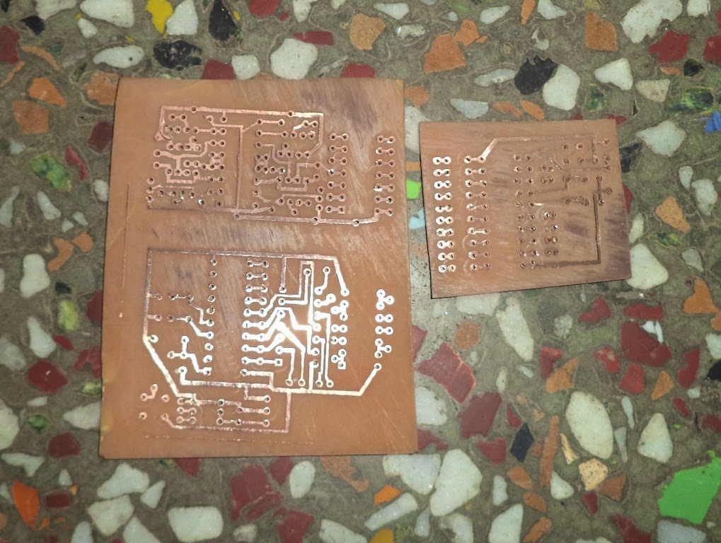
When Fifteen minutes has completed take out the pcb from the solution with the help of gloves and wash it with water.Now clean the pcb with thinner you Will notice that the extra copper has been removed and your pcb is ready for drilling.Drill the holes using hand drill or stand still drill at appropriate places where the components are to be placed. Use appropriate size of drill bit normally use 1mm bit.After drilling your pcb is ready to be used for placing components and shouldering.But before making the PCB layout of the circuit test the circuit on a breadboard.Here are the pcbs of the layout shown in this article.
Below is the H-Bridge circuit PCB.
Below is the Transmitter circuit PCB.
Below is the Receiver circuit PCB.
You can use the vast varieties of PCB designer software Only the difference lies is the operation of software but the procedure is same printing,transfering,eaching process etc. are same.Be careful with Ferric Chloride since it is highly corrosive.It is recommended to use gloves for treating with Ferric Chloride.


